
At SC21 (Supercomputing 2023), Intel hosted a short session the place they discussed their next-generation knowledge middle roadmap and talked about their upcoming Ponte Vecchio GPUs & the Sapphire Rapids-SP Xeon CPUs.
Intel Talks Sapphire Rapids-SP Xeon CPUs & Ponte Vecchio GPUs at SC21 – Additionally Reveals Subsequent-Gen Information Heart Lineup For 2023+
Intel had already mentioned many of the technical particulars concerning its next-gen knowledge middle CPU & GPU lineup at Sizzling Chips 33. They’re reaffirming what they’ve mentioned and in addition revealing a number of extra tidbits at SuperComputing 21.
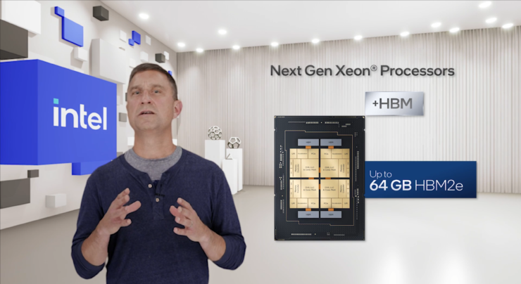
The present era of Intel Xeon Scalable processors has been extensively adopted by our HPC ecosystem companions, and we’re including new capabilities with Sapphire Rapids – our next-generation Xeon Scalable processor that’s presently sampling with prospects. This next-generation platform delivers multi-capabilities for the HPC ecosystem, bringing for the primary time in-package excessive bandwidth reminiscence with HBM2e that leverages the Sapphire Rapids multi-tile structure. Sapphire Rapids additionally brings enhanced efficiency, new accelerators, PCIe Gen 5 and different thrilling capabilities optimized for AI, knowledge analytics and HPC workloads.
HPC workloads are evolving quickly. They’re turning into extra various and specialised, requiring a mixture of heterogeneous architectures. Whereas the x86 structure continues to be the workhorse for scalar workloads, if we’re to ship orders-of magnitude efficiency beneficial properties and transfer past the exascale period, we should critically take a look at how HPC workloads are run inside vector, matrix and spatial architectures, and we should guarantee these architectures seamlessly work collectively.Intel has adopted an “complete workload” technique, the place workload-specific accelerators and graphics processing models (GPU) can seamlessly work with central processing models (CPU) from each {hardware} and software program views.
We’re deploying this technique with our next-generation Intel Xeon Scalable processors and Intel Xe HPC GPUs (code-named “Ponte Vecchio”) that can energy the two exaflop Aurora supercomputer at Argonne Nationwide Laboratory. Ponte Vecchio has the very best compute density per socket and per nodes, packing 47 tiles with our superior packaging applied sciences: EMIB and Foveros. There are over 100 HPC functions working on Ponte Vecchio. We’re additionally working with companions and prospects together with – ATOS, Dell, HPE, Lenovo, Inspur, Quanta and Supermicro – to deploy Ponte Vecchio of their newest supercomputers.
Intel Sapphire Rapids-SP Xeon Information Heart CPUs
In response to Intel, the Sapphire Rapids-SP will are available two bundle variants, a normal, and an HBM configuration. The usual variant will characteristic a chiplet design composed of 4 XCC dies that can characteristic a die dimension of round 400mm2. That is the die dimension for a singular XCC die and there will probably be 4 in complete on the highest Sapphire Rapids-SP Xeon chip. Every die will probably be interconnected by way of EMIB which has a pitch dimension of 55u and a core pitch of 100u.

The usual Sapphire Rapids-SP Xeon chip will characteristic 10 EMIB interconnects and the complete bundle will measure at a mighty 4446mm2. Shifting over to the HBM variant, we’re getting an elevated variety of interconnects which sit at 14 and are wanted to interconnect the HBM2E reminiscence to the cores.

The 4 HBM2E reminiscence packages will characteristic 8-Hello stacks so Intel goes for not less than 16 GB of HBM2E reminiscence per stack for a complete of 64 GB throughout the Sapphire Rapids-SP bundle. Speaking in regards to the bundle, the HBM variant will measure at an insane 5700mm2 or 28% bigger than the usual variant. In comparison with the just lately leaked EPYC Genoa numbers, the HBM2E bundle for Sapphire Rapids-SP would find yourself 5% bigger whereas the usual bundle will probably be 22% smaller.
- Intel Sapphire Rapids-SP Xeon (Customary Package deal) – 4446mm2
- Intel Sapphire Rapids-SP Xeon (HBM2E Package deal) – 5700mm2
- AMD EPYC Genoa (12 CCD Package deal) – 5428mm2
Intel additionally states that the EMIB hyperlink supplies twice the bandwidth density enchancment and 4 instances higher energy effectivity in comparison with normal bundle designs. Curiously, Intel calls the newest Xeon lineup Logically monolithic which signifies that they’re referring to the interconnect that’ll supply the identical performance as a single-die would however technically, there are 4 chiplets that will probably be interconnected collectively. You possibly can learn the total particulars concerning the usual 56 core & 112 thread Sapphire Rapids-SP Xeon CPUs right here.
Intel Xeon SP Households:
| Household Branding | Skylake-SP | Cascade Lake-SP/AP | Cooper Lake-SP | Ice Lake-SP | Sapphire Rapids | Emerald Rapids | Granite Rapids | Diamond Rapids |
|---|---|---|---|---|---|---|---|---|
| Course of Node | 14nm+ | 14nm++ | 14nm++ | 10nm+ | Intel 7 | Intel 7 | Intel 4 | Intel 3? |
| Platform Identify | Intel Purley | Intel Purley | Intel Cedar Island | Intel Whitley | Intel Eagle Stream | Intel Eagle Stream | Intel Mountain Stream Intel Birch Stream | Intel Mountain Stream Intel Birch Stream |
| MCP (Multi-Chip Package deal) SKUs | No | Sure | No | No | Sure | TBD | TBD (Probably Sure) | TBD (Probably Sure) |
| Socket | LGA 3647 | LGA 3647 | LGA 4189 | LGA 4189 | LGA 4677 | LGA 4677 | LGA 4677 | TBD |
| Max Core Rely | Up To twenty-eight | Up To twenty-eight | Up To twenty-eight | Up To 40 | Up To 56 | Up To 64? | Up To 120? | TBD |
| Max Thread Rely | Up To 56 | Up To 56 | Up To 56 | Up To 80 | Up To 112 | Up To 128? | Up To 240? | TBD |
| Max L3 Cache | 38.5 MB L3 | 38.5 MB L3 | 38.5 MB L3 | 60 MB L3 | 105 MB L3 | 120 MB L3? | TBD | TBD |
| Reminiscence Assist | DDR4-2666 6-Channel | DDR4-2933 6-Channel | Up To six-Channel DDR4-3200 | Up To eight-Channel DDR4-3200 | Up To eight-Channel DDR5-4800 | Up To eight-Channel DDR5-5600? | TBD | TBD |
| PCIe Gen Assist | PCIe 3.0 (48 Lanes) | PCIe 3.0 (48 Lanes) | PCIe 3.0 (48 Lanes) | PCIe 4.0 (64 Lanes) | PCIe 5.0 (80 lanes) | PCIe 5.0 | PCIe 6.0? | PCIe 6.0? |
| TDP Vary | 140W-205W | 165W-205W | 150W-250W | 105-270W | Up To 350W | Up To 350W | TBD | TBD |
| 3D Xpoint Optane DIMM | N/A | Apache Go | Barlow Go | Barlow Go | Crow Go | Crow Go? | Donahue Go? | Donahue Go? |
| Competitors | AMD EPYC Naples 14nm | AMD EPYC Rome 7nm | AMD EPYC Rome 7nm | AMD EPYC Milan 7nm+ | AMD EPYC Genoa ~5nm | AMD Subsequent-Gen EPYC (Put up Genoa) | AMD Subsequent-Gen EPYC (Put up Genoa) | AMD Subsequent-Gen EPYC (Put up Genoa) |
| Launch | 2017 | 2018 | 2020 | 2021 | 2023 | 2023? | 2024? | 2025? |
Intel Ponte Vecchio Information Heart GPUs
Shifting over to Ponte Vecchio, Intel outlined some key options of its flagship knowledge middle GPU similar to 128 Xe cores, 128 RT models, HBM2e reminiscence, and a complete of 8 Xe-HPC GPUs that will probably be related collectively. The chip will characteristic as much as 408 MB of L2 cache in two separate stacks that can join by way of the EMIB interconnect. The chip will characteristic a number of dies primarily based on Intel’s personal ‘Intel 7’ course of and TSMC’s N7 / N5 course of nodes.

Intel additionally beforehand detailed the bundle and die dimension of its flagship Ponte Vecchio GPU primarily based on the Xe-HPC structure. The chip will consist of two tiles with 16 lively dies per stack. The utmost lively prime die dimension goes to be 41mm2 whereas the bottom die dimension which can also be known as the ‘Compute Tile’ sits at 650mm2.
The Ponte Vecchio GPU makes use of 8 HBM 8-Hello stacks and comprises a complete of 11 EMIB interconnects. The entire Intel Ponte Vecchio bundle would measure 4843.75mm2. It is usually talked about that the bump pitch for Meteor Lake CPUs utilizing Excessive-Density 3D Forveros packaging will probably be 36u.

Apart from these, Intel additionally posted a roadmap wherein they affirm that the next-generation Xeon Sapphire Rapids-SP household and the Ponte Vecchio GPUs will probably be accessible in 2023 however there’s additionally the next-generation product lineup which is deliberate for 2023 and past. Intel hasn’t explicitly informed what it plans to carry however we all know that Sapphire Rapids successor will probably be often known as Emerald and Granite Rapids and the successor to that will probably be often known as Diamond Rapids.

For the GPU facet, we do not know what the successor to Ponte Vecchio will probably be identified however anticipate it to be competing with NVIDIA’s and AMD’s next-generation GPUs for the information middle market.
Shifting ahead, Intel has a number of next-generation options for superior packaging designs similar to Forveros Omni and Forveros Direct as they enter the Angstrom Period of transistor improvement.
Subsequent-Gen Information Heart GPU Accelerators
| Accelerator Identify | AMD Intuition MI200 | NVIDIA Hopper GH100 | Intel Ponte Vecchio |
|---|---|---|---|
| Packaging Design | MCM (Infinity Material) | MCM (NVLINK) | MCM (EMIB + Forveros) |
| GPU Structure | Aldebaran (CDNA 2) | Hopper GH100 | Xe-HPC |
| GPU Course of Node | 6nm | 5nm? | 7nm (Intel 4) |
| GPU Cores | 14,080 | 18,432? | 32,768? |
| GPU Clock Pace | 1700 MHz | TBA | TBA |
| FP16 Compute | 383 TOPs | TBA | TBA |
| FP32 Compute | 95.7 TFLOPs | TBA | ~45 TFLOPs (A0 Silicon) |
| FP64 Compute | 47.9 TFLOPs | TBA | TBA |
| Reminiscence Capability | 128 GB HBM2E | 128 GB HBM2E? | TBA |
| Reminiscence Clock | 3.2 Gbps | TBA | TBA |
| Reminiscence Bus | 8192-bit | 8192-bit? | 8192-bit |
| Reminiscence Bandwidth | 3.2 TB/s | ~2.5 TB/s? | 5 TB/s |
| Kind Issue | Twin Slot, Full Size / OAM | Twin Slot, Full Size / OAM | OAM |
| Cooling | Passive Cooling Liquid Cooling | Passive Cooling Liquid Cooling | Passive Cooling Liquid Cooling |
| TDP | This autumn 2023 | 2H 2023 | 2023-2023? |