
Santa Clara, California-based chipmaker Intel Company has gained an award from america Division of Protection (DoD) to develop a U.S.-based foundry ecosystem to fabricate semiconductors on modern chip course of nodes. This award is a part of the Pentagon’s Fast Assured Microelectronics Prototypes – Industrial (RAMP-C) program, which goals to counter the rise of Asian chip foundries with the event of chipmaking amenities inside america.
It goals to develop applied sciences able to fabricating transistors smaller than 7 nanometers – an area presently dominated by the Taiwan Semiconductor Manufacturing Firm (TSMC). Whereas the Pentagon remained silent in regards to the award, Intel introduced it via a press launch, highlighting that the Protection Division is within the firm’s 18A chip course of.
Intel Contract Highlights Pentagon’s Want For Superior Chipmaking Applied sciences
Intel’s 18A chip course of is a renamed model of what would seemingly have been its 2nm course of had the corporate not revamped its nomenclature earlier this yr. In July, the adjustments occurred when the corporate introduced its course of roadmap for the following 4 years and past.
Within the new roadmap, Intel renamed its superior 10nm Enhanced SuperFin chip course of as Intel 7 and dubbed its 7nm course of as Intel 4. Moreover, the corporate went past this to thoroughly change the best way it refers to its chipmaking applied sciences, because it launched two new nodes, dubbed because the 20A and 18A nodes.
These nodes, on the floor, try and wrench away the nomenclature advantaged loved by TSMC and Intel’s smaller rival, chip designer Superior Micro Gadgets, Inc (AMD). AMD has taken the ball to its bigger rival’s court docket by promoting 7nm processors, with Intel, on the floor, nonetheless sitting on 10nm chips.
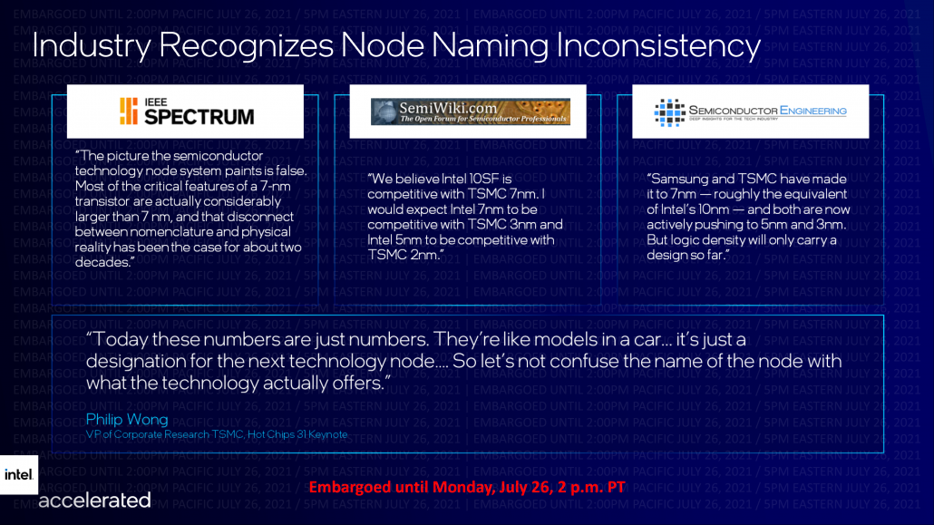
With exact particulars of the transistor densities and particularly dimensions of Intel 10nm and TSMC’s 7nm (utilized by AMD) unsure, the corporate, who was one of many first on this planet to undertake next-generation excessive ultraviolet (EUV) chipmaking machines, noticed itself wrestle to maintain tempo with each TSMC and AMD.

An Intel aspect from its course of roadmap revamp in July describing the discrepancies with modern-day chip course of nomenclature. Picture: Intel Company
Based mostly on our hypothesis, Intel’s 18A node, which has piqued the Pentagon’s curiosity, ought to resemble what beneath the older naming scheme could be known as a 2nm course of. The hypothesis follows logic, as 10 angstroms equal one nanometer, so 18 angstroms do find yourself roughly equal to 2 nanometers.
After all, and as Intel stresses within the slide above, even when the 18A course of is known as 2nm, this doesn’t indicate that its transistors are dimensionally much like equally named processes from different fabs.
What’s essential in terms of the 18A is the truth that Intel will use second-generation EUV machines to fabricate chips utilizing the method designs. These machines have a better numerical aperture (NA) and are merely known as Excessive-NA machines within the chip world.
Presently, TSMC employs precisely half of the worldwide put in production-ready EUV machines and has a lead in delivery processors constructed via them. Nevertheless, whereas entry to those machines is the primary a part of the chipmaking battle, entry to the high-NA machines would be the second.
With chipmakers going large and attempting to print transistors as high-quality as 5nm, 3nm and even 2nm, even the excessive wavelength ultraviolet mild might be pushed to its limits. To resolve this, the brand new machines will makes use of lenses with a 0.55 NA, which permits extra mild to move via than of their predecessors and permits for crisper transistor printing.
The 18A course of is anticipated to enter a degree of manufacturing by the second half of 2025, and if TSMC’s present tempo of analysis continues, then the corporate, like Intel, may also have shifted to a brand new transistor design within the race to squeeze billions of them in an area equal to a human fingertip