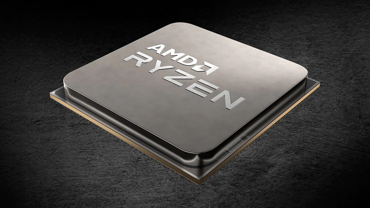

Just a few months in the past, AMD launched data on their new know-how for his or her Ryzen CPUs. AMD’s 3D V-Cache know-how takes as much as 64 megabytes of extra L3 cache & stacks it on prime of Ryzen CPUs.
AMD 3D V-Cache Stack Chiplet Design Additional Detailed, Ryzen 9 5950X With Boosted Sport Cache
Knowledge for contemporary AMD Zen 3 CPUs present that by way of their design to having the accessibility to permit for the 3D cache to be stacked from the start. This proves that AMD has labored on this know-how for a number of years.
Now, Yuzo Fukuzaki from the website TechInsights offers extra particulars about this new development in cache reminiscence for AMD. Offering a better look, Fukuzaki has discovered particular connection factors on the Ryzen 9 5950X pattern. There was additionally a be aware of extra house on the pattern that creates accessibility for the 3D V-cache by offering extra copper connection factors.

The stacking set up course of makes use of a know-how known as “through-silicon” vias, or TSV, which attaches the second layer of the SRAM to the chip by way of hybrid bonding. Utilizing copper for the TSV as a substitute of the standard solder permits for thermal effectivity and extra bandwidth. That is instead of utilizing solder to attach the 2 chips to one another.
He additionally notes in his LinkedIn article concerning the topic
To deal with #memory_wall drawback, cache reminiscence design is matter. Please take the chart in picture hooked up, Cache density pattern over course of nodes. In the most effective timing by economical causes, 3D reminiscence integration on Logic can contribute to have greater efficiency. See #IBM #Energy chips have large quantity of cache and powerful pattern. They will do it due to excessive finish server CPU. With #Chiplet CPU integration began by AMD, they will use #KGD (Recognized Good Die) to do away with low yield concern with monolithic giant scale die. This innovation has been anticipated at 2023 in #IRDS (Worldwide Roadmap Gadgets and Methods) Extra Moore and AMD will do it.

TechInsights delved deeper into how the 3d V-Cache connects, in order that they labored their approach by way of the know-how in reverse, and have offered the next outcomes with what was discovered, together with TSV data and the house contained in the CPU for the newer connections. That is the end result:
- TSV pitch ; 17μm
- KOZ measurement ; 6.2 x 5.3 μm
- TSV counts tough estimation ; about 23 1000’s!!
- TSV course of place ; Between M10-M11 (15 Metals in whole, ranging from M0)
We will solely speculate what AMD plans to make use of 3D V-Cache with its future buildings, such because the Zen 4 structure that’s to be launched within the close to future. This new know-how offers AMD processors an advantageous leap above Intel Expertise, as a result of L3 cache sizes turning into more and more essential as we see CPU core counts construct in measurement yearly.